Manipulating Material Properties of Atomic Layer Deposited Oxide Thin Films by Electric Field: Experimental and Computational Design (ALDBIAS)
Topic
The ALDBIAS project follows both technological and fundamental scientific objectives. On the technological side, ALDBIAS targets the advancement of plasma-enhanced (PE) atomic layer deposition (ALD) by applying an electric field (BIAS) to tailor the material properties at an atomic level. The scientific objective of the project is the profound understanding of relationships between material properties and factors influencing PEALD synthesis of thin oxide films, both with and without bias. The working hypothesis of ALDBIAS is that electric field can influence properties of PEALD synthesized materials by two mechanisms:
(i) Depending on the bias, electric field may increase or lower energy transfer between plasma sheath and the surface due to acceleration or deceleration, respectively, of the bombarding ions.
(ii) Assuming partially ionic character of the material electric field creates an additional force Fi = qi E, on each atom in the oxide layer, where qi is the partial atomic charge and E the electric field strength.
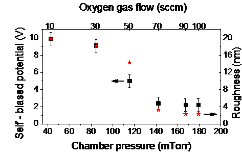
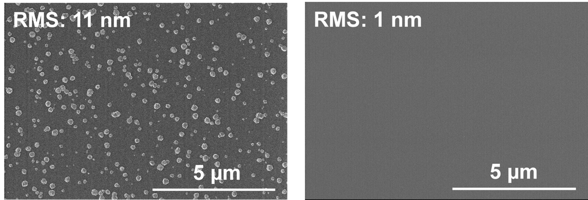
Energetic ions bombarding the surface can influence most material properties like refractive index, stress, transmission, crystallinity, thin film density. Ion – surface interaction can lead to various effects which are augmented by an external electric field: adatom migration, atomic peening, surface implantation or subplantation, interdiffusion in nanolaminates and composite materials, desorption or re-sputtering. The correlation between the roughness of TiO2 PEALD thin films and the self-bias potential is presented in Fig. 1. and Fig. 2 shows SEM images if the coating grown without and with an external electric field.
Contact Person(s)
Prof. Dr. Marek Sierka | Dr. Adriana Szeghalmi |
|---|---|
Friedrich-Schiller University Jena Otto Schott Institute for Material Research (OSIM) | Friedrich-Schiller University Jena Institute of Apllied Physics (IAP) |
Löbdergraben 32 07743 Jena | Albert-Einstein-Str. 15 07745 Jena |
Tel: (+49) 3641 9 47930 | Tel: (+49) 3641 9 47859 |
Fax: (+49) 3641 9 47792 | Fax: (+49) 3641 9 47802 |
Proj.-Nr. SI 938/8-1 | Proj.-Nr. SZ 253/2-1 |